A Hybrid CMOS Digital-to-Analogue Converters Design for High Resolution SAR ADC
DOI:
https://doi.org/10.37934/araset.32.3.121138Keywords:
Digital-to-Analogue Converter, high resolution, hybrid architecture, linearity, low powerAbstract
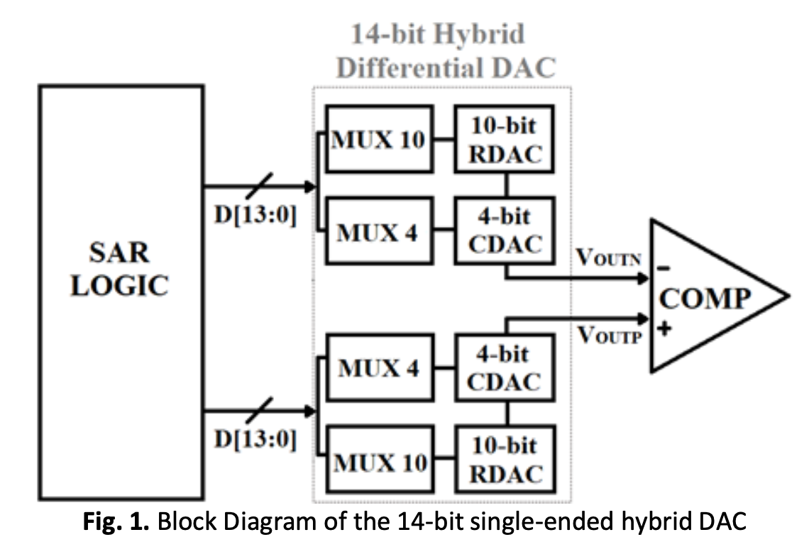
The paper describes the design and implementation of a 14-bit differential Digital-to-Analogue Converter (DAC) based on the Silterra 0.18µm Complementary Metal-Oxide-Semiconductor (CMOS) process to be established in a Successive Approximation Register (SAR) Analogue-to-Digital Converter (ADC) for the purpose of high-resolution, high accuracy and low power applications. The proposed differential DAC aims to eliminate the issue of stringent matching requirements imposed on high-resolution DACs while leveraging both linearity performance and power consumption parameters at a balanced point. The overall differential circuit consists of two parallel single-ended DACs that utilize a 4-bit Capacitor DAC (CDAC) and 10-bit Resistor DAC (RDAC) on each end, thereby establishing a hybrid-based architecture. Furthermore, the authors illustrate the proposed switching procedures applied to the sub-DAC circuits to ensure a low-power design is established. The new method effectiveness evaluation is confirmed by detailed transient simulations implemented on the DAC where the circuit performs the required conversions at a maximum conversion frequency of 2.5 MS/s with a peak power consumption of 0.1496mW for the standard voltage supply of 2.1V. Meanwhile, the schematic and post-layout simulations performed on the DAC registers peak DNL errors of -0.1612 and -0.8272, respectively. New research results depict performance improvements in terms of resolution and power consumption which facilitates the DAC implementation in contemporary electronic devices such as microcontroller peripherals and audio amplification devices. The overall deigned circuit is capable of achieving the desired 14-bit digital-to-analogue conversions under the CMOS 0.18µm technology, proving the DAC’s high-resolution efficacy.
Downloads
