A Numerical Approach for Predicting Temperature Distribution, Heat Flow, and Material Deformation of Printed Circuit Board during Laser Soldering
DOI:
https://doi.org/10.37934/aram.112.1.4656Keywords:
Laser soldering, thermal distribution, heat flow, printed circuit boardAbstract
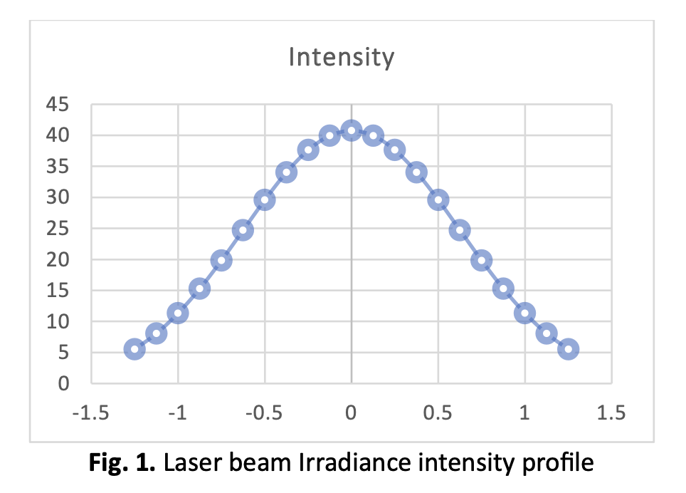
This paper presents a numerical simulation approach using the finite element method (FEM) in ANSYS software to overcome the limited accessibility of laser soldering machines which are expensive. The study aims to examine the viability of simulating a laser soldering process using ANSYS steady-state thermal simulation. The simulation aims to produce accurate predictions for temperature distribution, heat flow, and deformation of the material during the process. A Gaussian laser beam equation is used to analyse the interaction between the laser beam and metallic components, particularly on PCB boards. This paper evaluates the properties of a laser beam and the Sn-3.0Ag-0.5Cu (SAC305) lead-free solders which are commonly used in electronic industries. As a result of the thermal analysis, the temperature distribution within the solder spots, as well as the copper as printed circuit board (PCB) can be determined, whereas the mechanical analysis of the materials can be determined by looking at their deformation and stress in the system. The results show that the laser beam effectively contains heat within the solder contacts, reducing the risk of excessive heat transfer. The copper acts as an efficient heat sink, managing thermal energy during the process. However, the solder point experiences substantial deformation and stress, indicating potential limitations in its performance. Nonetheless, the neighbouring components and solder joints exhibit a factor of safety, ensuring the overall safety and reliability of the system.
Downloads
