A Review of Moldflow and Finite Element Analysis Simulation of Chip Scale Packaging (CSP) for Light Emitting Diode (LED)
DOI:
https://doi.org/10.37934/arfmts.99.1.158173Keywords:
Chip scale packaging, light emitting diode, computer aided engineeringAbstract
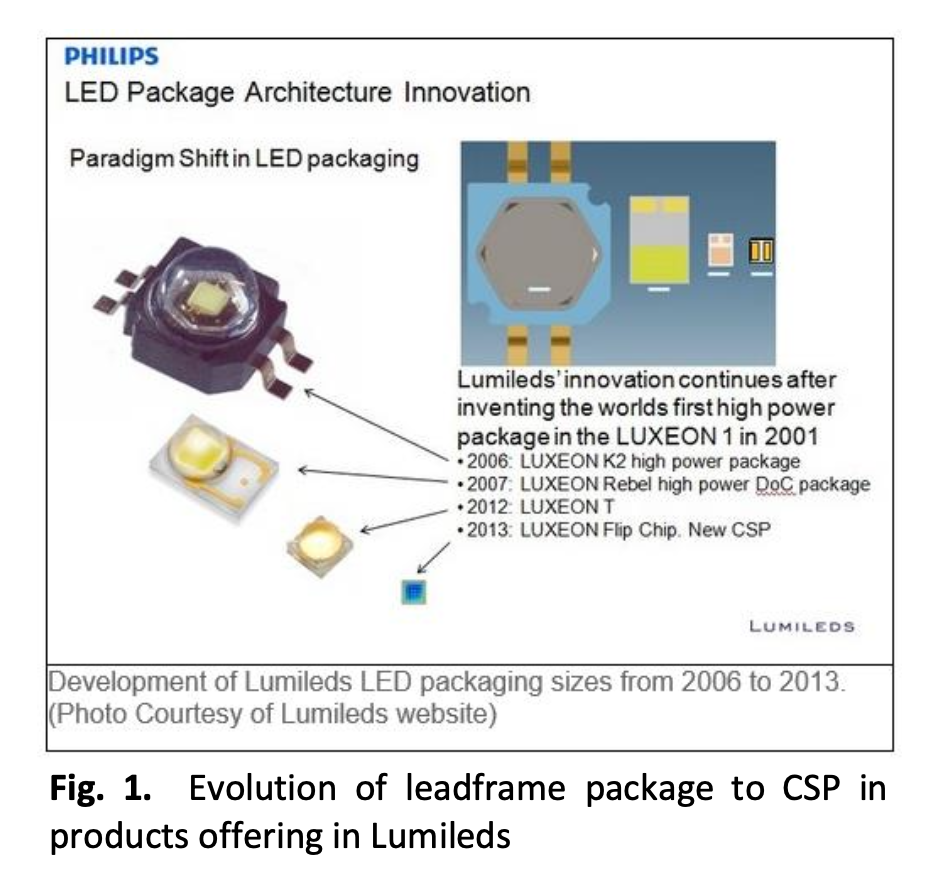
LED technology has been evolving aggressively in recent years from incandescent bulb during older days to as small as chip scale package. There is tremendous pressure to stay competitive in the market by optimizing products to next level of performance and reliability with shortest time to market. This changes the conventional way of product design and development to virtual prototyping by means of Computer Aided Engineering (CAE). The objective of the paper is to review challenges in chip scale packaging application in LED technology. The first part of the paper covered the literature survey of Chip Scale Packaging (CSP) in Light Emitting Diodes (LED), CSP architecture challenges, molding process and material for CSP. The findings of literature found that very few researchers had study silicone encapsulations process in CSP for LED in term of material characterization, mold process and simulation. Findings also shows that deployment Computational Fluid Dynamic (CFD) and integration of virtual prototyping using Finite Element Analysis (FEA) in product development in CSP for semiconductor industry had greatly reduced the time to market. However, there are very few papers discuss the application for CSP technology in LED industry. Second objective of the papers is discussion of methodolology in molding material characterization and simulation methodology. CFD helps to simulate the flow pattern of molding material as a function of different temperature, molding parameters settings for voids and displacement. FEA also help to evaluate the deformation of silicone in panel form and enable designer to predict the displacement of devices with different silicone.
Downloads
Downloads
Published
How to Cite
Issue
Section